susie@jxgreentape.com
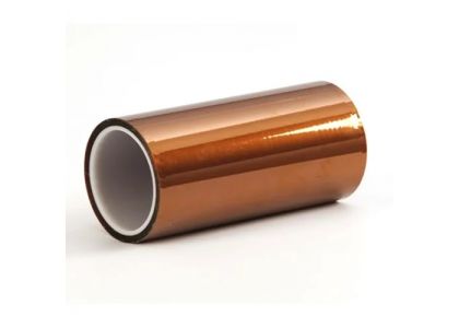
Protecting semiconductor chips from mechanical damage, ESD, moisture, and thermal stress is a day-to-day problem across packaging, logistics, and assembly. In practice, Premium quality kapton tape is often used as a controlled, temporary process material—especially for masking, fixture hold-down, and surface protection—because polyimide film maintains dimensional stability at elevated temperature and supports clean removal when the adhesive system is correctly matched.
For engineering teams evaluating materials, the real decision is rarely “Kapton or not,” but which construction (film thickness, adhesive chemistry, liner type) survives your exposure window without residue or lifting. This guide summarizes the most common failure modes, how to validate tapes under realistic conditions, and how Buy kapton tapes decisions can be de-risked through sampling and pilot trials rather than relying on generic claims. It also clarifies when “Best polyimide tape” and Customized PI tape (die-cuts, slits, alignment features) make sense for repeatable semiconductor workflows.
Semiconductor packaging and handling environments impose constraints that are easy to underestimate when tapes are treated as generic consumables. In many chip workflows, the main risks are not film burn-through, but process-related issues such as:
Residue contamination: Flux residue interaction, adhesive transfer after heat exposure, or residue that interferes with conformal coating / testing contacts.
ESD risk: Tape itself is not an ESD control method unless the overall handling system (liners, trays, grounding, humidity control) is designed accordingly.
Cleanroom compatibility: Outgassing, particle generation, and ionic contamination can become limiting factors in sensitive packaging steps.
Edge lift and creep: Thermal cycling plus mechanical handling can trigger edge lift, which then exposes surfaces that were meant to be protected.A critical point often missed in semiconductor discussions is that Kapton tape is typically used as a temporary process aid, not a permanent packaging material. Treating it as a permanent barrier can introduce long-term reliability risks that the material was never intended to address.
Polyimide film (Kapton) is valued in semiconductor operations because it tolerates high process temperatures, resists many commonly encountered solvents, and provides strong dielectric performance. In transport and assembly steps, Kapton tape is commonly used for:temporary masking of sensitive pads/leads during soldering, coating, or cleaning steps
holding small packages in fixtures during automated handling
creating temporary barriers between components to reduce scuffing or contact damage
supporting controlled removal after defined process windowsCompared with generic masking tapes, process-grade constructions typically provide more consistent peel behavior, better dimensional stability under heat, and fewer residue-related surprises—provided the adhesive chemistry is compatible with the substrate and exposure profile.
In semiconductor manufacturing, Kapton tape is typically qualified as a temporary process material, and its suitability is verified through application-specific testing rather than generic datasheet values.
Common validation steps include:
Thermal exposure testing
Tape samples are exposed to the maximum process temperature and dwell time expected during transport or assembly (e.g., pre-bake, reflow adjacency, or burn-in handling). After exposure, peel behavior and residue are evaluated.
Adhesion and clean removal checks
Engineers assess whether the tape can be removed cleanly from substrates such as silicon, ceramics, metals, or FR-4 without adhesive transfer. This step is critical for downstream inspection and electrical testing.
Chemical compatibility screening
Short-term contact with flux residues, cleaning solvents, or humidity-controlled environments is simulated to confirm that adhesive performance remains stable.
Outgassing and cleanliness considerations
For cleanroom or sensitive packaging steps, low-outgassing grades and compatible liners are verified to avoid contamination risks.Rather than assuming that all polyimide tapes behave similarly, these tests help confirm whether a specific construction performs reliably within the defined process window.
Choosing the correct Kapton tape for semiconductor use involves matching material construction to the actual handling and assembly conditions.
Key selection factors include:
Customization for repeatability
Customized PI tape, such as die-cut masks or pre-slit formats, can significantly reduce manual handling and improve consistency when the same masking or protection pattern is used repeatedly.
The following examples illustrate typical, realistic use cases without relying on unverifiable performance claims.
Transport protection for high-value devices
In multi-site semiconductor logistics, Kapton tape is often used to immobilize components within trays or carriers. Process-grade constructions help minimize surface scuffing and contact damage during vibration and handling, provided adhesive tack is matched to ambient conditions.
Thermal fixture handling during burn-in
Kapton tape is frequently used to secure devices in burn-in trays where elevated temperatures are present. Low-outgassing polyimide constructions help maintain clean contact surfaces and avoid contamination during extended thermal exposure.
Precision masking during assembly
In die attach or packaging steps, Customized PI tape die-cuts are applied to protect bond pads or sensitive regions. Pre-shaped masks reduce manual trimming, lower handling errors, and improve process repeatability across shifts.
These examples highlight how Kapton tape supports process control when used within its intended, temporary role.
To use Kapton tape effectively in semiconductor transport and assembly, a structured approach is recommended:Define the thermal profile, handling stresses, and chemical exposure involved.
Shortlist candidate tapes based on film thickness, adhesive type, and cleanliness requirements.
Validate performance through small-scale trials that replicate real process conditions.
Evaluate Best polyimide tape options based on repeatability and clean removal, not on generic “premium” labels.
When you Buy kapton tapes in volume, retain tested reference samples and request batch consistency documentation.Investing in Premium quality kapton tape is most effective when material selection is driven by process validation rather than assumptions. When correctly chosen and applied, Kapton tape becomes a predictable control element that protects chips, stabilizes assembly steps, and helps maintain yield across transport and manufacturing operations.