susie@jxgreentape.com

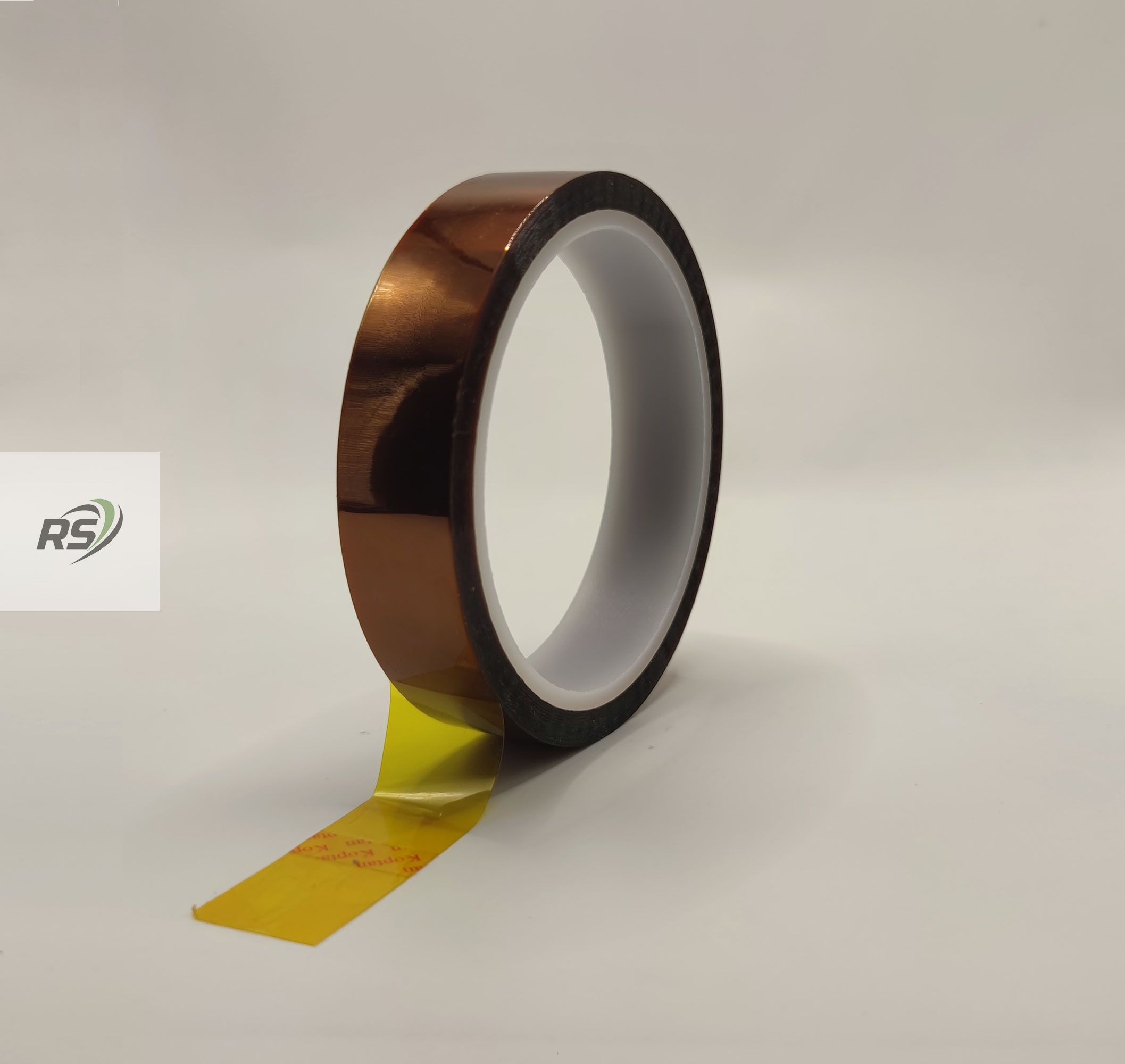

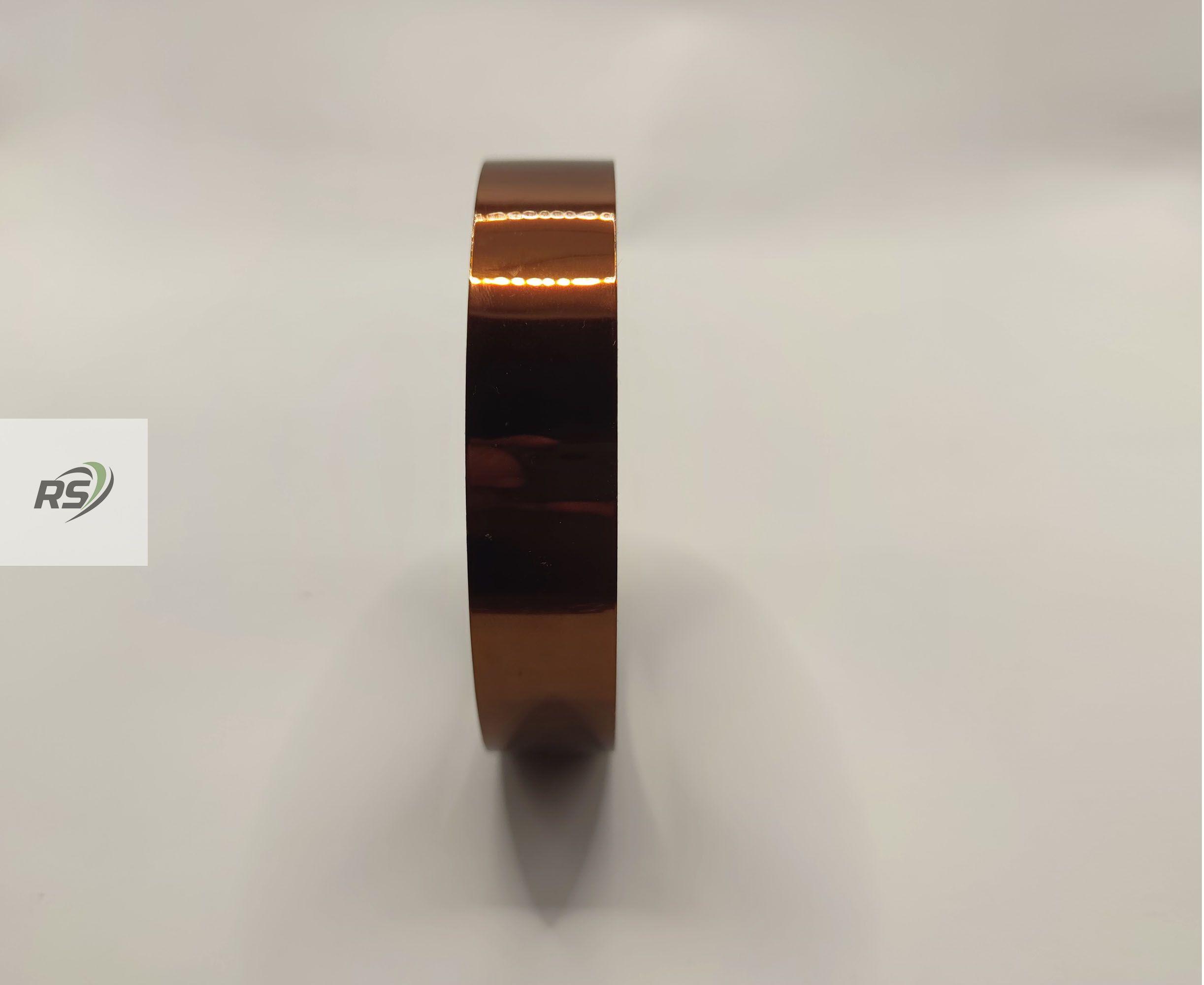
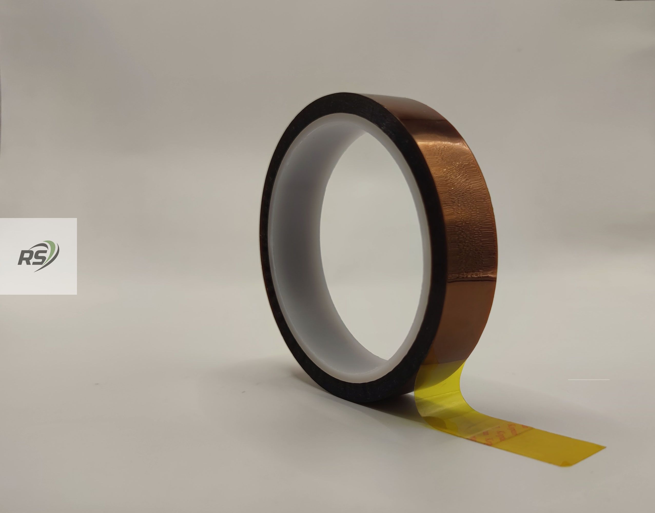
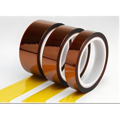
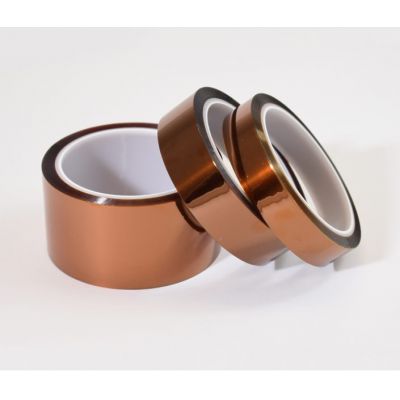
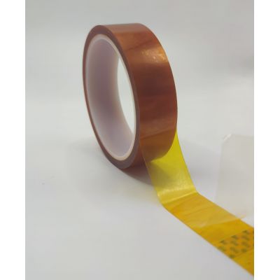
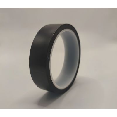
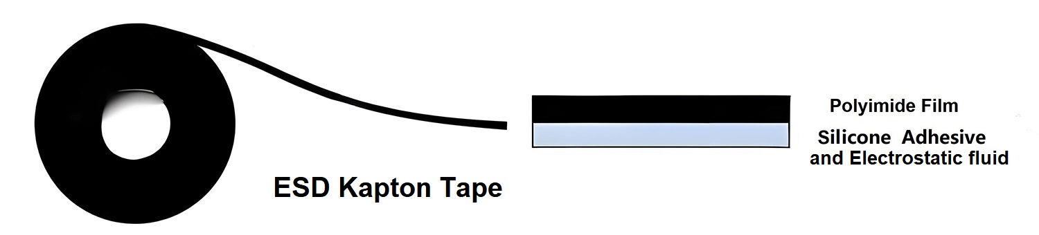
J-630A ESD Kapton Tape is a low-static polyimide adhesive tape designed for electronic masking, PCB protection, SMT assembly, semiconductor-related handling, and high-temperature insulation work where ordinary polyimide tape may generate unwanted electrostatic charge during unwind or removal. It uses polyimide film backing with silicone pressure-sensitive adhesive and is available in standard rolls, custom widths, and die-cut shapes. Typical surface resistance is 10^6–10^9 Ω based on product specification, but actual ESD behavior should be confirmed under the buyer’s handling method, humidity, substrate, and removal speed.
Standard Kapton-style tape is already known for heat resistance and electrical insulation, but that is not always enough in electronics production. In PCB masking, gold finger protection, SMT assembly, and semiconductor-related operations, the tape may be peeled near sensitive ICs, connectors, and mounted components. That removal step is where static charge becomes a real concern.
J-630A ESD Kapton Tape is designed for buyers who need the familiar benefits of polyimide tape, but with better static-control behavior during process masking and removal. It is not a magic fix for every ESD problem in a factory. It should still be used inside a proper ESD control process. The value is more specific: it helps reduce the risk that masking tape itself becomes a charge-generation source during PCB and electronics assembly.
If your project involves solder masking, gold finger protection, or selective electronic process masking, our PCB and electronics masking solutions page gives a wider view of where polyimide, polyester, and other masking tapes fit.
|
Item No. |
Film Thickness |
Total Thickness |
Adhesion to Steel |
Tensile Strength |
Heat Resistance |
Elongation at Break |
Surface Resistance |
|
J-630A |
0.025 mm |
0.06 mm |
5.5 N/25mm |
10 kg/25mm |
260°C |
45% |
10^6–10^9 Ω |
|
J-630A |
0.05 mm |
0.08 mm |
5.5 N/25mm |
20 kg/25mm |
260°C |
55% |
10^6–10^9 Ω |
Data should be treated as typical product information unless otherwise confirmed in the final TDS, test report, or purchase specification. Heat resistance, residue behavior, and ESD performance can change with dwell time, pressure, substrate, storage, humidity, and removal method. Test methods, tolerances, and batch values should be confirmed before production approval.
The surface resistance range matters because ESD-sensitive production is not only about whether the tape is insulating. A tape may have good dielectric properties but still create charge during unwind or peeling. For PCB masking or semiconductor-related handling, buyers should ask how the ESD value is tested and whether low charging during removal has been evaluated.
Thickness is another practical detail. The 0.06 mm version is useful when fine masking lines, lower edge buildup, and easy conformability are important. The 0.08 mm version gives stronger handling and higher tensile strength, which may help when operators need easier removal or when the tape is applied over slightly rougher areas.
Adhesion to steel is useful for comparison, but PCB laminates, gold fingers, connectors, plastic films, and battery tabs are not steel. Do not approve a tape only from a catalog adhesion value. Test it on the actual surface after the actual heat cycle. If your team is comparing adhesive systems, our Kapton tape silicone adhesive and Kapton tape acrylic adhesive pages can help clarify why heat resistance, residue, and silicone-contact risk are not the same question.
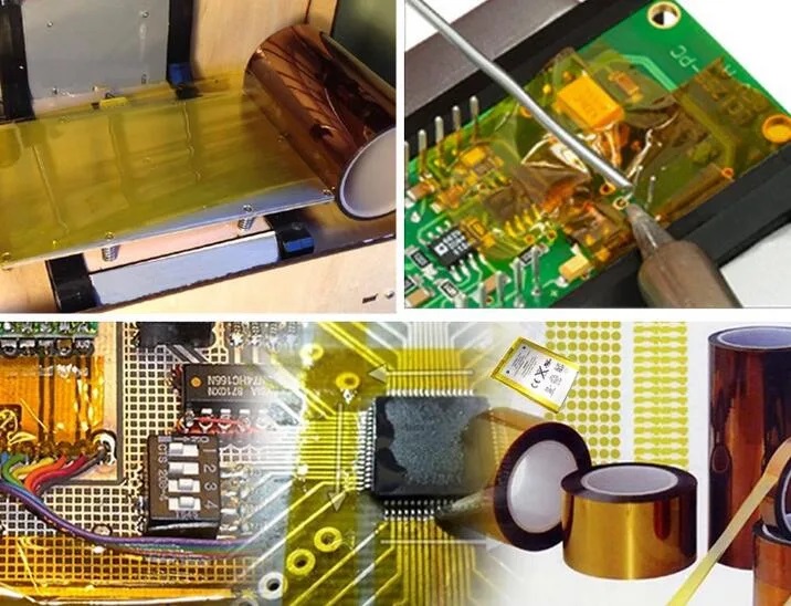
The strongest use case for J-630A is electronic process masking where both heat resistance and static control matter. Typical applications include PCB gold finger masking, wave solder protection, reflow soldering protection, connector masking, SMT process masking, selective conformal coating masking, and die-cut protection parts for electronic assembly.
For PCB gold fingers, the main concern is usually edge sealing and clean removal. The tape must stay flat enough to stop solder or flux from entering the protected area, but it should not leave adhesive transfer after heating. For SMT and semiconductor-related operations, buyers should also consider charge generation during tape unwind and peel-off.
In battery pack assembly, ESD Kapton tape may be used for temporary tab fixation, local insulation, and heat-resistant masking, but battery applications should be validated carefully. Electrolyte exposure, pressure, aging, and cell design can change the result. For motor, coil, or transformer-related insulation support, buyers should confirm dielectric data and long-term temperature exposure before approval.
For applications mainly involving bonding, mounting, or insulation layer lamination rather than removable masking, double sided Kapton tape may be the better product family. If the requirement is visual contrast, light shielding, or low-glare inspection rather than ESD control, black Kapton tape may be more relevant.
A few applications need extra caution. Low-surface-energy materials such as PP, PE, PTFE, and silicone rubber should still be tested before approval. Silicone adhesive may perform better on silicone rubber than acrylic adhesive, but release agents, silicone oil, dust, surface migration, and process conditions can still change the result.
Conformal coating is another area where buyers should slow down. Silicone adhesive can be useful for heat resistance and removal, but any possible silicone transfer should be checked if coating wetting or bonding follows later. A surface can look clean and still create coating defects. If your current masking tape leaves residue, lifts at the edge, or causes coating problems, review our tape failure analysis before simply switching to another tape with the same temperature rating.
Medical, optical, aerospace, and vacuum-related uses should not be approved from this product page alone. Those applications may require additional tests such as outgassing, optical cleanliness, sterilization compatibility, or customer-specific qualification. J-630A can be sampled for evaluation, but special-use approval belongs to the buyer’s validation process.
ESD control is not defined by one number only. Surface resistance, charge generation during unwind, charge generation during removal, grounding, humidity, operator method, and the actual substrate all affect risk. A low-static tape should be assessed as part of the full ESD control environment, not as a standalone guarantee.
For B2B qualification, buyers may request surface resistance data, charge-generation data during unwind or removal if available, and batch consistency information. If the customer follows an ESD control program, the tape should be reviewed under that program’s material control requirements.
J-630A is designed to reduce static risk during masking and removal, but we do not recommend treating any tape as universally ESD-safe for every semiconductor or precision electronics process without validation.
We supply J-630A in standard roll formats and can slit to custom widths for PCB assembly, connector masking, battery tab work, and electronic component protection. Width control matters more than many buyers expect. A tape that is even slightly too wide may interfere with nearby pads or inspection points; a tape that is too narrow may allow flux or coating to enter the protected area.
For repeated masking positions, die-cut ESD Kapton parts can improve consistency. They reduce hand-cutting, improve alignment, and help operators apply the same geometry across batches. Die-cut parts can be supplied with release liner, tab design, sheet format, or roll format depending on the application.
For broader sourcing decisions, including material comparison, adhesive choice, and sample approval steps, our industrial tape buying guides provide a useful starting point.
Before requesting a sample, send more than width and length. The most useful information includes application position, process temperature, dwell time, substrate, removal timing, ESD requirement, residue requirement, thickness target, roll size, and whether die-cutting is needed.
For PCB masking, include the protected area, soldering method, and whether conformal coating or cleaning follows later. For battery or motor insulation, include the surface material, pressure, expected aging condition, and whether the tape is temporary or permanent. For ESD-sensitive lines, tell us whether the concern is unwind, removal from PCB, handling near components, or all of them.
This saves time. It also avoids the common mistake of approving a tape that looks good at room temperature but fails after heat, pressure, or real production handling. If you are still comparing ESD Kapton tape with standard polyimide, polyester, or other high-temperature tapes, our material comparisons page can help narrow the choice.
What is the difference between ESD Kapton tape and standard Kapton tape?
Standard Kapton-style tape focuses mainly on high-temperature masking and insulation. ESD Kapton tape adds static-control treatment or construction features to reduce charge generation during unwind or removal. Buyers should still confirm surface resistance and removal behavior under their own process conditions.
Can ESD Kapton tape be used for PCB gold finger masking?
Yes, PCB gold finger masking is one of the common applications. The tape should be tested for edge holding, heat resistance, clean removal, and static behavior after the actual wave solder or reflow process. Do not approve it only from room-temperature adhesion data.
Does ESD Kapton tape leave residue after high-temperature soldering?
Clean removal depends on adhesive type, dwell time, temperature profile, substrate, pressure, and removal timing. J-630A is designed for clean removal under suitable process conditions, but buyers should validate residue performance on the real PCB or component before bulk approval.
Is the surface resistance 10^6–10^9 Ω guaranteed for every use condition?
The listed range is product specification data, but actual ESD behavior can be affected by test method, humidity, substrate, handling speed, and storage. For controlled production, request the applicable test report or confirm the value as part of your incoming quality check.
Can you provide custom die-cut ESD Kapton tape?
Yes. We can provide custom widths and die-cut shapes for PCB layouts, connectors, battery tabs, insulation pads, and other electronic masking parts. Send drawings, tolerance requirements, liner format, packaging method, and sample quantity for review.
Should I choose silicone adhesive or acrylic adhesive Kapton tape?
Silicone adhesive is often used for higher temperature masking and soldering-related processes. Acrylic adhesive may be considered where non-silicone contact, lower silicone-transfer concern, or specific cleanliness requirements matter. The right choice depends on heat cycle, substrate, residue limit, and downstream process.
Request a Sample for Your Process
Send your PCB process condition, soldering profile, substrate, thickness target, ESD requirement, and residue standard. We can review your application and recommend a J-630A roll or die-cut sample configuration for validation, instead of sending only a generic sample roll.
For distributors, OEM buyers, and electronics assembly plants, we can support custom width slitting, die-cut converting, bulk packaging, private-label requirements, and product data documentation upon request.