susie@jxgreentape.com
Gold fingers (edge-plated contact pads) are a premium, wear-sensitive part of many PCBs used for docking, connectors, or card-edge interfaces. During wave solder, molten solder, flux residues, and mechanical abrasion can damage the gold plating or leave contamination that later causes poor contact or accelerated wear. Using the right masking solution avoids rework and reduces warranty risk.
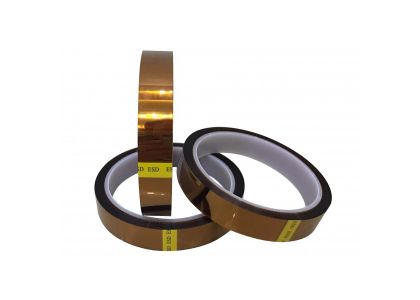
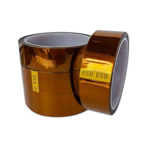
One proven solution in production lines is ESD Kapton tape for PCB masking: polyimide film with an antistatic surface and a heat-resistant adhesive layer that survives typical wave-solder temperatures while enabling clean removal after the process.
Polyimide film (Kapton-type) is stable up to the ~250–260°C range used in wave-solder processes. The ESD-treated surface prevents triboelectric charging during handling, reducing particulate attraction and ESD risks. Important properties for gold-finger protection:
Backing: polyimide film, thin and conformable so it follows board edge contours.
Temperature rating: continuous exposure and short spikes up to ~260°C.
Adhesive: silicone or high-temp acrylic chosen to balance tack with clean removability.
ESD surface: controlled surface resistivity to avoid introducing charges.
When you source tape, request technical data sheets that include tack values, adhesion (N/cm or oz/in), peel at 90° after heat exposure, and surface resistivity.
Scenario: A contract manufacturer (CM) assembles a PCIe-style controller with 14 gold fingers per edge. Previously, occasional solder bridging and flux residue required hand-cleaning and re-polishing, increasing cycle time.
Action taken:
Masked the gold-finger area with a 12 mm wide ESD Kapton tape rolls for SMT chosen for conformability.
Used a silicone adhesive variant to allow 30–60 minutes post-solder dwell before removal.
After wave solder at 255°C, operators removed the tape parallel to the finger direction; no adhesive smear, no plating damage, and zero bridging in masked areas.
This example highlights why choosing the right tape width and adhesive system matters as much as the polyimide backing.
Practical, reproducible results come from process discipline:
Mask application: press down with a roller to ensure full contact — gaps or bubbles are potential entry points for flux.
Overlap and edge treatment: avoid overhangs that create lift; trim excess with a sharp blade.
Solder temperature control: maintain wave set points and conveyor speed to reduce unnecessary thermal stress on adhesive.
Dwell time before removal: allow the assembly to cool to a safe handling range recommended by your supplier (typical recommended wait is 10–30 minutes depending on adhesive). Removing too soon can stretch adhesive or leave residue; removing too late (many hours) can increase adhesion and risk partial transfer.
Removal technique: pull at a low angle (≤30°) and parallel to the gold fingers to peel without stressing the plating.
Before approving material in your line, perform a simple incoming-batch test:
Test protocol (example):
Mount sample board with representative gold-finger pad finish.
Apply tape strips (same width used in production).
Run one pass through a test oven or solder simulator at production peak temperature (e.g., 255°C for 20–30 seconds exposure).
Allow controlled cool-down (e.g., 20 minutes).
Peel at a fixed speed and angle; assess for: residue, cohesive failure, adhesive transfer, or plating damage.
Measure peel force if available. Record results in the incoming QC report.
This approach lets you quantify behavior across batches from an ESD Kapton tape supplier or direct factory shipments. Keep a control sample on file so future lots can be objectively compared.
Failure mode: adhesive residue on gold fingers after removal.
Fix: switch to a silicone adhesive variant or shorten post-solder dwell time; perform solvent compatibility checks and improve operator removal technique.
Failure mode: tape lifts during wave, allowing solder ingress.
Fix: improve application pressure, verify board handling prior to solder, or move to a higher tack grade while monitoring removability.
Failure mode: tribocharging attracts flux/particles to masked edge.
Fix: ensure supplier provides an antistatic surface or choose factory direct anti static kapton tape grades with controlled surface resistivity.
When evaluating sources — from an ESD kapton tape manufacturer or through distributors — ask for:
Technical Data Sheet (TDS) with temperature rating, peel strength before/after heat, and surface resistivity.
Sample availability in production widths (for example, 6 mm, 12 mm, 18 mm).
Batch traceability and certificate of conformity.
Recommended removal window and recommended storage conditions.
Lead time and MOQ for ESD Kapton tape rolls for SMT and options for custom slit widths.
Case studies or references from other electronics assemblers.
A disciplined supplier selection reduces line trials and keeps your first-pass yield high.
Actionable checklist to implement today:
Order 3 candidate samples from a reliable ESD Kapton tape supplier (one silicone adhesive, one high-temp acrylic, one medium tack).
Run the incoming-batch test described in section 5.
Standardize operator removal procedure (angle, speed, dwell time).
Add tape TDS and test records to your process control documents.